这篇文章转载自我在eetop上的文章
常见缩写词
LVS : layout versus schematic
DRC: design rules check
DFM: design for manufacturability
PERC: programmable electrical rules check
PEX: post extract
LPE: layout post extract
RVE: results viewing environment
SAB: silicide (salicide自对准硅化物) blocking layer
SAB is the salicide block layer. The source/drain or polysilicon overlapped by SAB will not be salicided and is relatively high resistive. If you don’t draw it, the resistor’s resistance value will decrease dramatically.
OD:oxide diffusion
和AA(active area)一样,都是有源区。
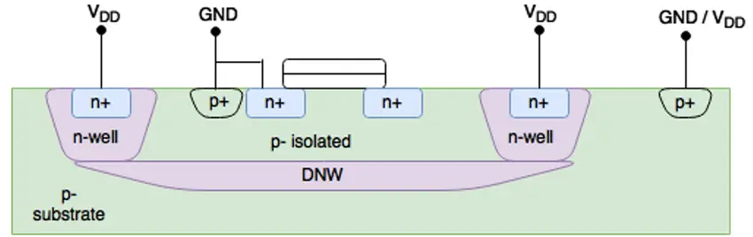
DNW: Deep N Well [1]
NT_N: Native Layer
使用这一层后,硅衬底变为不掺杂,电阻率约10 Ω·cm。否则为默认低掺杂,约0.1-1 Ω·cm。 在有些工艺中,这一层叫做PSUB。
DMY: dummy
SVT: standard threshold voltage(一般用于标准阈值电压器件)
LVT: low threshold voltage
HVT: high threshold voltage
UHVT: ultra high threshold voltage
ULVT: ultra low threshold voltage
ckt: circuit
chk: check
subckt : sub-circuit 子电路
OPA/OPAMP/OA: operational amplifiers 运算放大器
参考文献
–
- Dragan, Anca & Negut, Alina & Enache, A. & Anghel, Vlad & Brezeanu, G.. (2018). Charge retention of a floating gate transistor for a reset controller. Romanian Journal of Information Science and Technology. 21. 34-48.